


Kyocera establishes Additive Manufacturing of SiSiC components in Germany

Kyocera Fineceramics Europe GmbH, a division of Japan’s Kyocera, has expanded its high-performance ceramics portfolio with the addition of a silicon carbide Additive Manufacturing process, developed at its Selb, Germany, facility.
“The introduction of Additive Manufacturing is a milestone for our company,” stated Dr Carsten Russner, president of Kyocera Fineceramics Europe. “It brings up new potential for us in terms of development and application as well as strategic positioning in the market.”
Silicon-infiltrated silicon carbide (SiSiC) is a high-performance ceramic material known for its exceptional mechanical strength, thermal conductivity, rigidity and high wear resistance. SiSiC is well suited to demanding areas of application such as aerospace, the semiconductor industry and industrial production, particularly due to its barely measurable thermal expansion. Kyocera processes both StarCeram Si, which is used for conventional manufacturing processes, and StarCeram AM-Si, which was developed for Additive Manufacturing independently; both materials are characterised by comparable material properties.
As the technology progresses, Additive Manufacturing has been increasingly adopted in the production of complex SiSiC components. Compared to traditional shaping processes such as isostatic pressing, slip casting or film casting, AM offers greater design freedom and shorter development cycles. For example, topology-optimised components can be produced, which can lead to significantly reduced weight. Ceramic Additive Manufacturing can be used as a solution for demanding designs where conventional techniques reach their limits.
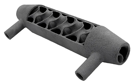
The multi-stage production process was specially developed for large-volume and complex components. The maximum component size is 325 x 270 x 130 mm with wall thicknesses from 3 mm. The elimination of green machining, programming times and the manufacture of tools for machining enable particularly short production times and volume production.
Using this technology, Kyocera offers its customers a portfolio of components from prototype development to series production. The process is generally based on a two-stage procedure:
- A green part is created from silicon carbide powder and polymer binder using the Binder Jetting (BJT) AM process
- The part is infiltrated with molten silicon, which reacts with the remaining carbon to form the final SiSiC structure
“This advancement is the result of intensive research and development work,” explained Sarah Diener, Team Leader for Additive Manufacturing. “We look forward to creating added value for our customers through the production of complex component geometries.”
Kyocera also offers design consultancy for the optimisation of component geometries and the implementation of topology-optimised structures. Working with customers, the component weight can be reduced or the performance of the components increased. The company works in close cooperation with its own design centre to provide customers with tailor-made solutions.
“Additive Manufacturing enables us to react flexibly to dynamic market requirements,” stated Dr Nikolaos Katsikis, Director Research & Development. “We see great added value for our customers, particularly when it comes to large and complex components – especially when we are able to provide optimisation support through our design consulting.”
Alongside its materials offerings, Kyocera offers post-processing and coating technologies that expand the range of applications for additively manufactured components. The company’s Selb location is a comprehensive manufacturer of SiSiC components and is therefore specialised in furnace technology for large-volume components, the final processing of the material, as well as joining experience and coating technologies.
europe.kyocera.com
www.kyocera.com