


Copper micro-structures made by NIL/micro-SPiMIM
Researchers at Kinki University, Osaka Prefectural College of Technology, and Taisei-Kogyo Co Ltd, reported at PM2010 on a process called NIL/µ-SPiMIM to produce micro-structures having a 5µm to 10µm fine line and space pattern for use as optical fibre connectors, micro-impellers, micro-reactors, etc. As with the technology used to produce micro-heat sinks from Cu-diamond composites also developed at Osaka Prefectural College of Technology and reported in the June 2010 issue of PIM International, the researchers adopted their sacrificial plastic mould (SP-mould technology) into which are inserted polymethylmethacrylate (PMMA) films made by thermal nanoimprint lithography (NIL) techniques. The PMMA films produced by NIL can have line and space (L/S) pattern structures with dimensional accuracy of the order of nanometers, and micro-structures of just a few microns.
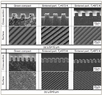
Fig. 1 SEM images of green and sintered micro-patterned parts
produced from nano Cu powder. From paper by K. Nishiyabu
etal, published in Proceedings of PM2010 World Congress,
Florence, 10-14 October
The researchers stated that their thermal NIL process consists of three steps; 1) Heating the PMMA film to above the glass transition temperature, 2) pressing and cooling to transcribe the Si-mould shape to the PMMA film, and 3) de-moulding the film from the Si-mould. The subsequent μ-SPiMIM process involves three further steps; injection moulding of MIM feedstock into the SP-mould; ejecting the green compacts and SP-mould as one component, removing the SP-mould; and solvent debinding the polymeric binders followed by sintering at 973K in Ar+20%H2 gas to achieve the desired sintered density.
The materials used for producing the injection moulding feedstock for the micro-structured MIM parts are pure copper powder and polyacetyl based binder. The nano-sized copper powder is manufactured commercially by a wet-reduction method (Fukuda Metal Foil & Powder Co. Ltd.) and has a mean diameter: D50=0.7μm, tap density: ρa = 3.17 g/cm3, specific surface area: Sv = 1.69 m2/g).
Fig. 1 shows the SEM images of green and sintered parts processed at 573K and 973K. In the green compacts with both L/S = 5μm and 10μm, the researchers found that the feedstock has seemingly filled the micro-channels completely, but the polymer binder builds up at the upper corners of microscopic structures. The sintered parts processed at 573K have many sub-micron pores, because both debinding and oxidising have not been completed at this lower temperature. However, it was found that the sintered parts processed at 973K keep the edge sharpness under optimised debinding and sintering conditions.