


Cooling the limits of power electronics: An integrated approach for e-mobility and AI hardware with copper MIM
As power density continues to rise in applications ranging from e-mobility to AI hardware, thermal management is increasingly defining the performance limits of power electronics. Conventional cooling concepts are struggling to keep pace, making system-level optimisation essential. This article presents a coordinated approach to substrate design, high-current interconnection and advanced copper cooling enabled by Metal Injection Moulding, developed jointly by Schweizer Electronic AG, Schunk Sonosystems GmbH and Schunk Sintermetalltechnik GmbH, and authored by Marvin Luceri, Thorsten Klein and Tim Hanika. [First published in Powder Injection Moulding International Vol. 20 No. 1, Spring 2026 | 10 minute read | View on Issuu | Download PDF]
Cooling has long been a central challenge in power electronics. Rising power levels and power density are driving ever-higher thermal loads, making thermal management one of the key limiting factors in system performance.
Two developments are driving this trend. First, the transformation towards e-mobility is progressing rapidly: as charging power increases and charging times shorten, vehicles face steadily rising power requirements, resulting in growing thermal loads that must be managed reliably for safety reasons. Second, similar effects are evident in AI hardware, where increasing power density means conventional airflow-based heat removal is no longer sufficient; in extreme cases, systems may be forced to throttle chip clock speeds to prevent overheating.

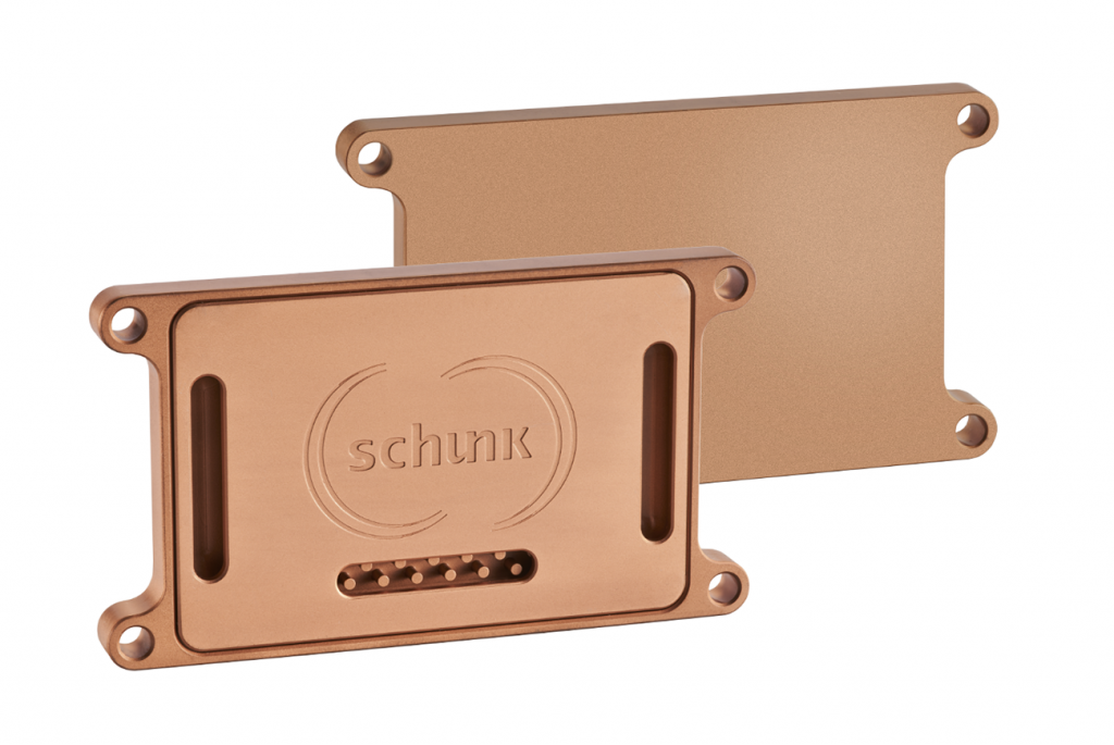
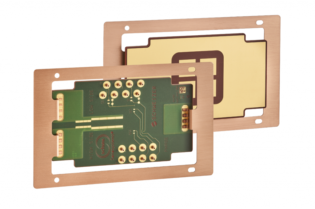
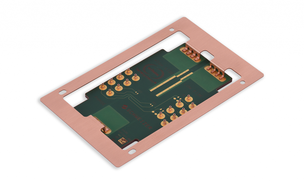
Three companies have joined forces in a development consortium to address the challenge of efficient heat dissipation in high-power electronics: Schweizer Electronic AG, a specialist in high-power PCB technology, Schunk Sonosystems GmbH, with expertise in ultrasonic-welded high-current busbar connections, and Schunk Sintermetalltechnik GmbH, a leading manufacturer of components produced by Metal Injection Moulding. Using a joint reference build (Figs. 1 and 2), the companies demonstrate how coordinated design of substrate, interconnection, and cooling can improve thermal performance and overall system efficiency.
This system approach places requirements on all three subsystems: the PCB substrate, the high-current interconnections, and the cooling component. One key element of the overall concept is the cooling component, which must combine high thermal conductivity with design freedom. MIM copper is particularly suitable for such applications, as its sintered microstructure achieves near-full density and thermal conductivities approaching wrought copper. Combined with the ability to form thin walls, hollow structures, and intricate internal features without machining, this enables compact, highly efficient cooling geometries.
Component selection must therefore consider not only the thermal transport properties of the base material, but also mechanical stability under coolant pressure and compatibility with joining processes (such as ultrasonic welding and pressure sintering to the PCB). This requires controlled surface conditions, uniform acoustic impedance and tight tolerances to ensure stable energy transfer and robust metallurgical bonding to the PCB structures.

Validation typically requires a combination of pressure testing, flow characterisation, thermal resistance measurement, and non‑destructive evaluation methods, such as X-ray computed tomography (CT) scanning or scanning acoustic microscopy (SAM), to verify internal structural conformity – including confirmation that the cooler’s internal pin-fin posts (heat-transfer features) are fully connected to the base plate.
High-power PCB substrates and integration
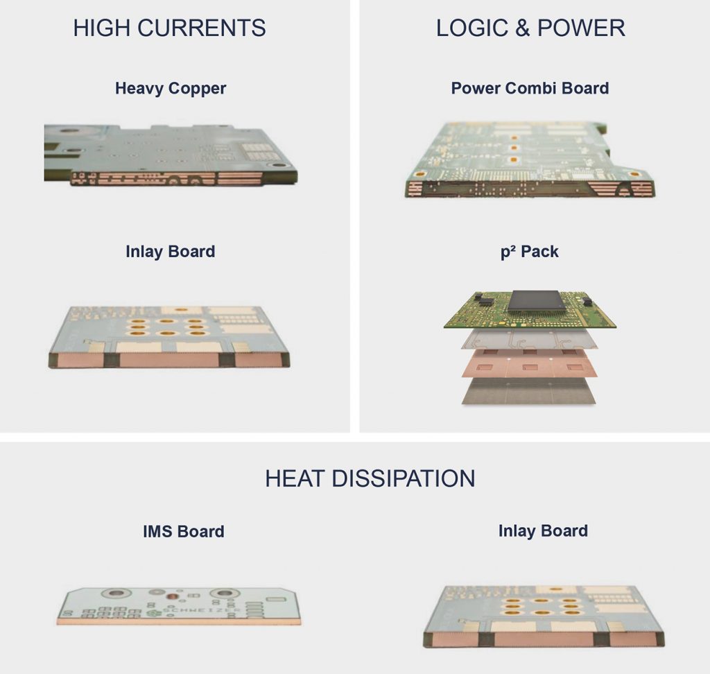
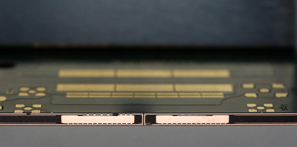
Modern power PCB technologies, such as standard, clustered or etched inlays, thick-copper circuit boards and highly integrated embedding approaches, provide far more than simple electrical interconnection (Fig. 3). Owing to their high copper content, these substrates act as active thermal components within the system. They buffer short-term load and current peaks while simultaneously enabling efficient heat conduction from the power semiconductor to the underside of the printed circuit board, making the PCB itself a key element of thermal management. In the demonstrator, busbars were attached directly to the PCB by ultrasonic welding, implemented by Schunk Sonosystems GmbH.
As currents increase, conventional contacting and interconnection solutions quickly become the limiting factor. Contact resistance and parasitic inductance directly affect efficiency, electromagnetic compatibility (EMC) performance and service life. System-optimised high-current connections with short, wide-area current paths ensure that the electrical advantages of the PCB are preserved all the way to the power semiconductor.
Regardless of the PCB’s thermal capability, heat must be removed from the system efficiently. Closed copper heat sinks manufactured using MIM technology offer advantages here. MIM enables highly complex geometries with integrated cooling channels and large surface areas, while still supporting high-volume production. Directly coupling such heat sinks to the underside of the PCB reduces thermal interfaces and simplifies the overall system design.
System-level improvements demonstrated in the reference build
The impact of the integrated system approach described here can be demonstrated particularly clearly using highly integrated demonstrators. One such reference is the p² Pack model from Schweizer Electronic AG (Figs. 4 and 5), which integrates power semiconductors directly into a copper-based substrate.
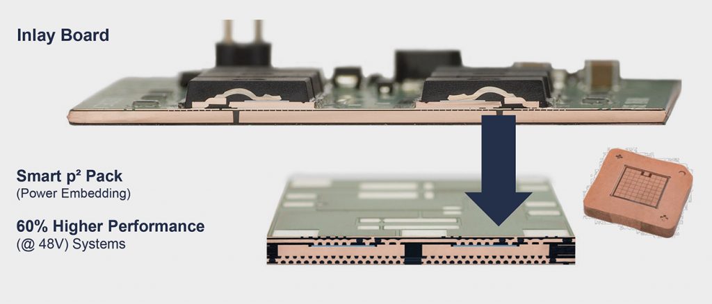
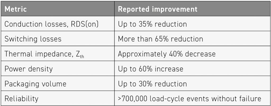
Although this approach is not the primary focus of the article, it enables the system-level effects to be quantified. In the p² Pack reference design, the following improvements have been reported (Table 1). These results highlight the potential that emerges when the PCB, current paths, contacting, and cooling are designed consistently as an integrated whole. Depending on the level of integration, these effects can also be transferred to inlay or thick-copper PCBs.
The cooler solution
Metal Injection Moulding offers design freedom similar to plastic injection moulding and is therefore suitable for producing components at medium- and large-scale volumes. The process begins with a very fine metal powder (<45 µm) – typically high-purity copper for high-performance heat conductors – which is mixed with a binder system to form a feedstock. At injection temperature, the feedstock has a viscous, paste-like consistency and can be processed on standard injection moulding machines. The feedstock is melted and injected under high pressure into precisely manufactured mould cavities.
The moulded component (‘green part’) is then debound; the polymer binder used to hold the metal powder together during moulding is removed, leaving a porous metal skeleton in the shape of the final part. Debinding is typically carried out by solvent debinding, catalytic debinding, thermal burnout, or some combination thereof. The resulting so-called ‘brown part’ consists of loosely bonded metal particles and maintains the shape and dimensions of the green part.
The component is then sintered under a protective gas atmosphere or vacuum at temperatures close to the melting point of the metal. During sintering, diffusion causes the brown part to shrink and densify into a high-density, low-porosity structure. Although the component typically shrinks linearly by 10-20% during sintering, dimensional accuracy remains high due to the homogeneous density of the green compact and the controlled process conditions. The result is a precise, functional metal part.
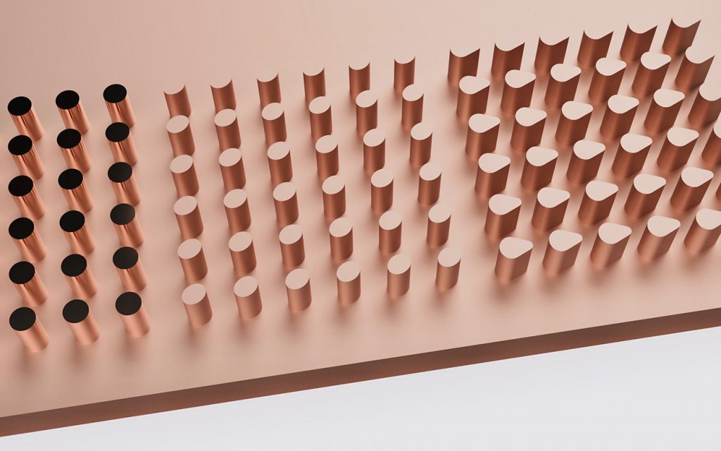
From a thermal-fluidic perspective, the cooler’s internal geometry governs the balance between heat transfer efficiency and hydraulic performance. Dense pin arrays or structured surfaces significantly increase internal surface area, while alternative pin morphologies – such as tapered, oval, or hemispherical shapes – can induce microscale turbulence, reduce the thermal boundary layer thickness, and thereby enhance convective heat transfer. At the same time, the design must mitigate excessive pressure drop to preserve overall system efficiency. Ensuring uniform coolant distribution is essential to avoid localised thermal gradients and hotspot formation within the copper structure.
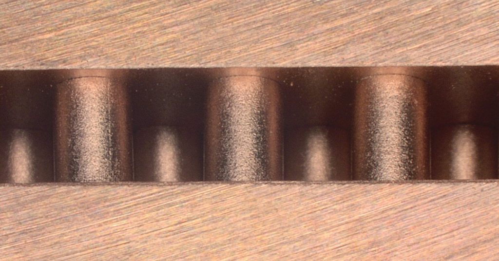
Special process variants enable MIM to produce hollow heat-exchanger structures for the cooler (Figs. 6 and 7), designed for operation with glycol-water mixtures at pressures of up to 8 bar. Cylindrical pins were used to keep tooling costs down. The pins connect both base plates. This ensures optimal heat conduction from the heat source to the cooling medium, including through the second cover plate (with maximum surface area). Alternatively, the cooler can dissipate heat on both cover plates and thus be used on both sides. The water pipe connections are provided as mounting elements in step one; in step two, they can be directly moulded during the forming process.
Pure copper has excellent thermal conductivity. With optimised powder quality and tightly controlled sintering, modern MIM copper can achieve high density and therefore high thermal conductivity, approaching that of fully dense copper.
The economic appeal of copper heat sinks produced using MIM is based on several factors. First, MIM enables complex internal cooling geometries – such as integrated channels and structured surfaces – that would be prohibitively expensive to machine in copper. Second, MIM eliminates material-intensive removal processes, which are particularly cost-relevant for copper. With high material utilisation, MIM achieves favourable raw material efficiency. In addition, the use of recycled material contributes to a favourable CO2 balance.
Ultrasonic welding for high-current interconnections
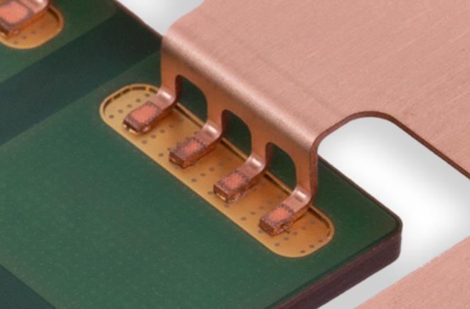
Electrical currents and signals must ultimately be transferred from the inner structures of the PCB to the outside of modern power modules. This is where ultrasonic welding can be applied as a joining method (Fig. 8).
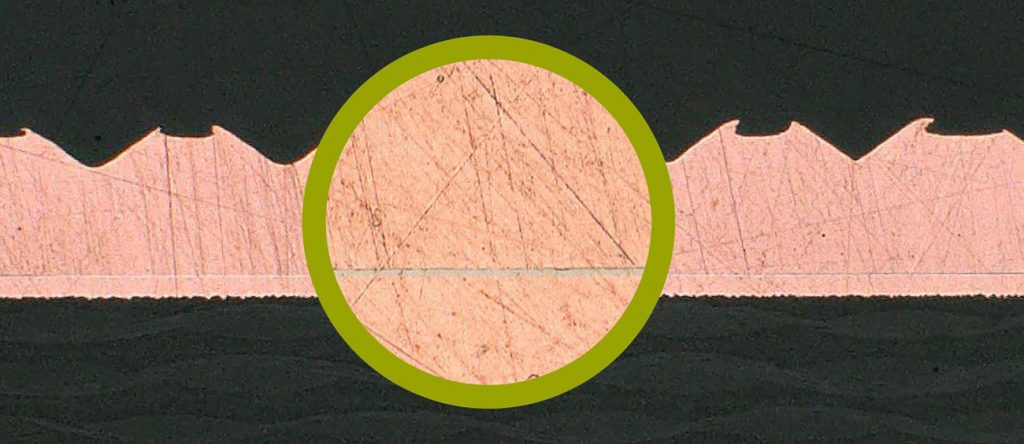
Ultrasonic welding is a solid-state joining process in which mechanical vibrations in the high-frequency range – usually between 20–40 kHz – are introduced into the joining zone under defined force. The sonotrode transfers the vibration energy to the material surfaces, causing microscopic relative movements. These lead to local friction, plastic deformation and breakdown of oxide layers, resulting in metallic contact at the atomic level and the formation of a material bond (Fig. 9). Since the process does not require external heat input, it is classified as a cold joining process.
Principles and advantages
Key advantages of ultrasonic welding include very short process times in the millisecond range and high reproducibility of joint quality. Energy input can be precisely controlled, making the process particularly suitable for sensitive assemblies. This technology also enables the joining of different metallic materials, including combinations with widely varying thermal and mechanical properties. The resulting joints exhibit high electrical and mechanical stability, making the process particularly suitable for applications in electronics manufacturing, sensor technology, and power electronics.
Process parameters and challenges
Ultrasonic welding of PCBs and MIM coolers involves specific process requirements. Key parameters include amplitude, welding force, welding time and energy input. The amplitude determines the intensity of the vibrations and thus the degree of plastic deformation in the joining zone. The welding force ensures the necessary surface contact, while the welding time and energy input influence the resulting weld intensity and material deformation.
The combination of sensitive PCB laminates for contacting and MIM components as heat sinks and bases poses a particular challenge. When ultrasonic welding on very thin conductor layers, there is a risk that excessive amplitudes or forces will lead to delamination, conductor track detachment or local overheating on the printed circuit board. Geometric tolerances and variations in surface finish also significantly impact process stability.
Optimised tool and sonotrode geometry; suitable component positioning and joining; and continuous process monitoring are therefore required for reliable process control. Modern ultrasonic systems use high-resolution sensors and correspondingly high sampling rates to monitor process variables and parameters such as energy input, force curve and frequency, thereby improving reproducibility and joint quality.
Summary
Thermal management is increasingly setting the limits for high-power electronic assemblies. Joint development work by Schweizer Electronic AG, Schunk Sonosystems GmbH, and Schunk Sintermetalltechnik GmbH highlights the value of treating the substrate, interconnection, and cooling as a single integrated design task – particularly at the interfaces, where joint quality, surface conditions, and tolerances directly affect both electrical losses and heat transfer.
Looking ahead, further qualification of these integrated concepts will be essential to scaling power density in applications such as e-mobility and AI hardware, while maintaining efficiency and reliability.
Contact
Marvin Luceri
Strategic Marketing Manager
[email protected]
+49 7422 512-206
Schweizer Electronic AG
Einsteinstrasse 10, 78713 Schramberg, Germany
www.schweizer.ag
Thorsten Klein
Head of MIM – Schunk Thale
[email protected]
+49 3947 7-1560
Schunk Sintermetalltechnik GmbH
Rosstrappenstrasse 62, 06502 Thale, Germany
www.schunk-group.com
Tim Hanika
Head of Special Applications
Schunk Sonosystems GmbH
[email protected]
+49 641 608-347
Hauptstrasse 95, 35435 Wettenberg, Germany
www.sonosystems.com