


Ceramics in new dimensions: Additive Manufacturing at CeramTec
No matter which market report you choose to believe, all recent analysis of the ceramic AM market points to major growth. But this is still an emerging technology, and in terms of its commercial development, ceramic AM is said to be five years behind metal AM. Now, as global manufacturers of high-performance ceramics enter the market, an even faster acceleration in technology adoption is promised. Here, Claus Falkner, of CeramTec, a producer of technical ceramics by processes that include Ceramic Injection Moulding, explores the benefits of ceramic Binder Jetting and considers the process as a compelling solution for complex parts. [First published in PIM International Vol. 16 No. 2, June 2022 | 10 minute read | View on Issuu | Download PDF]

CeramTec, headquartered in Plochingen, Germany, ranks among the largest international manufacturers of ceramics for technically demanding applications. The company began its Additive Manufacturing journey in 2015 with the aim of building up a division for the production of ceramic components. Owned by CPP Investment Board Europe S.àr.l, and BC Partners as of August 2019, CeramTec reported an annual turnover of almost €553 million ($592.2 million) in 2020, despite the difficult market situation created by COVID-19, and currently employs around 3,400 staff at twenty production sites in Europe, North and South America, and Asia. This article will highlight CeramTec’s AM capabilities and present the Binder Jetting (BJT) process as a compelling production solution for ceramic parts.
For CeramTec, the decision to invest in an in-house ceramic AM unit in 2015 ties in deeply with the company’s strategy of diversification in all business areas, as well as its DNA of innovation. A dedicated and continued focus on R&D has been at the core of the business since its beginnings in the early 20th century, with customer requirements and the ability to provide added value in a rapidly changing market space the key guidelines for development.
When the company first began integrating its ceramic AM capabilities, a technical centre was set up at its Lauf site in Bavaria to develop the process, from BJT to the final component, including thermal treatment with a final sintering process and optional surface finishing.
Innovations in silicon carbide ceramics
At the beginning of 2021, CeramTec’s BJT process for the production of parts in a specific technical ceramic material was officially launched, enabling the business to combine the special material properties of silicon carbide ceramics (SiSiC) with the advantages of the relatively fast, cost-effective BJT process.
SiSiC is a versatile, two-component material comprising a metallic phase with silicon, making it electrically conductive and affording it a range of beneficial properties including superior rapid cooling, rapid heat resistance, wear resistance, oxidation resistance, high bending strength and a long service life. It also has excellent hard-wearing properties and is not only the lightest, but also the hardest ceramic material. It stands out for its thermal conductivity and has virtually no thermal expansion. The latter is particularly important for the semiconductor industry, which uses SiSiC wafer chucks in chip production.
Most importantly, this material demonstrates very little shrinkage during the sintering process, retaining relatively stable dimensions, which also makes it suitable for extremely large components such as structural parts for machines or nozzles, for example in the chemical industry. For CeramTec, the decision to work with binder jetted SiSiC, which allows for the production of lightweight components with particularly high stiffness and strength, enabled a wide range of interesting applications. The company’s in-house developed SiSiC material, ROCAR®3D, is the result of a fine-tuning process which optimised the properties of additively manufactured SiSiC components in such a way that the material characteristics correspond to the properties of conventionally manufactured components to within a few percentage points.
The process: ceramic Binder Jetting
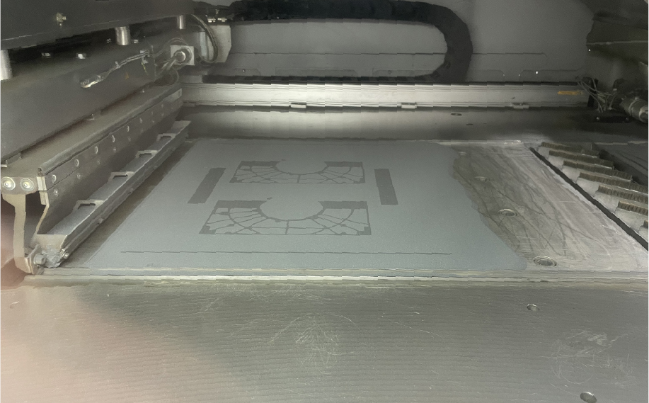
The original Binder Jetting process was developed through an MIT (Massachusetts Institute of Technology) project in the late 1980s. The principle is similar to laser sintering for metal, but uses a jetted binder – instead of a laser beam – to ‘weld’ the material together. Essentially, structures are manufactured through the application of droplets of liquid binding agent (phenolic resin) in a very fine jet onto a powder bed of ceramic powder grains to weld them together in the pattern defined by the STL file. Layer by layer, this process is repeated until a ceramic green body is obtained, which then undergoes sintering to obtain ceramic properties.
Binder Jetting is one of the most scalable AM technologies and is being used to produce big components from a variety of materials, including ceramics. It has a number of advantages such as scalability, design freedom and throughput. With material thickness from 2 mm to 35 mm and hole diameters from 2 mm, ceramic design options are wide ranging. One key benefit is that BJT works without support structures. The self-supporting powder bed enables the production of geometrically complex parts as they are required by CeramTec’s customers. This can, for example, include the AM of parts containing internal cavities, such as cooling channels, which can even be curved.
As SiSiC is significantly lighter than steel, the process also lends itself to lightweight construction. Through the use of clever design for BJT, similar part strengths and structural properties to those of steel parts can be achieved with far less weight in SiSiC. In the future, as energy efficiency becomes more important, this will become ever more relevant in the industrial context. An example of high-value applications are rotating components – such as pump impellers – which have traditionally been made of steel. Being able to deploy a much lighter ceramic rotating component means that less energy has to be applied to drive the part. The larger such rotating components become, the bigger an issue part weight presents, making ceramic a very interesting option – and ceramic AM is key to opening up these new fields of application where ceramic has previously not been used.

While CeramTec currently uses its AM facilities primarily for the development and production of prototypes, starting with a batch size of one, and components in small series, the BJT process was also chosen with a view to scalability and ease of replicating the current AM unit at the company’s Lauf site in other production facilities. The overall Binder Jetting mechanism enables speed and a considerable fabrication throughput, based on the technology working by laying down a layer of ceramic powder at once and the advantage of depositing the binder using an inkjet-like buildhead. This is a fast process that can easily be scaled up when using several jetting heads to increase throughput.
In ongoing process development, CeramTec is also looking at how to partially automate Binder Jetting to make the process, which in its current form requires significant manual work between its individual production steps – namely the removal of parts from the powder bed – even more efficient.
Case study: SiSiC for heating
Harnessing the advantages of AM, such as enabling fast delivery times for small quantities and sophisticated geometries, CeramTec uses ceramic Binder Jetting to produce heating elements for several applications such as welding and drying.
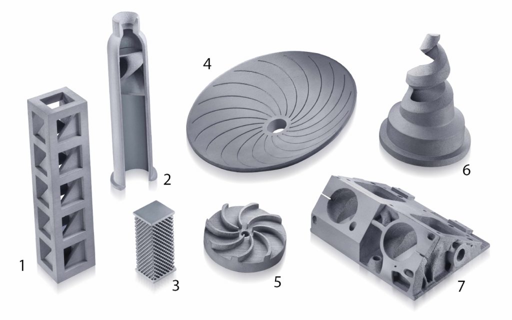
Crucially, these parts take advantage of the specific properties of SiSiC (i.e., the combination of high thermal and electrical conductivity with other characteristics of high-performance ceramics, namely high hardness and chemical resistance). Since emitters need to be manufactured for each product specifically, they require a wide range of complex geometries in small quantities, making them an ideal application for AM as a flexible, customisable production technology. As no set-up costs are incurred, the cost-effective production of individual pieces or small series can easily be supported. In the unlikely event of a failure, the use of AM means that an exact replacement is available at short notice.
Further ceramic AM applications
SiSiC is also a key material for semiconductor manufacturers due to its extremely low thermal expansion. Photolithography systems for semiconductor manufacturing are becoming more sophisticated and component suppliers need to be able to provide products of the highest quality to meet the current and future demands in chip production.
In 2020, the global semiconductor industry recorded a turnover of $440 billion, driven by increasing digitalisation of the products we use every day, and developments in the technologies around artificial intelligence, 5G, emobility and the internet of things, which all rely on semiconductor technology.
In recognition of the demand for semiconductors, the European Commission launched the ‘European Alliance on Processors and Semiconductor Technologies’ in July 2021. The aim of the alliance is to increase the European share of global semiconductor production to 20% by 2030 and to expand manufacturing capacity to develop state-of-the-art semiconductor chips in the 5–2 nanometer range.
CeramTec has long-standing expertise in manufacturing SiSiC plates which are used as the basis for electrostatic wafer chucks in semiconductor machines for the production of chips and AM enables the company to act as an innovative partner for its customers in this industry. The flexible design options offered by AM are key here as SiSiC components can be produced in unique product geometries that are not supported by other manufacturing processes.
Ongoing integration of ceramic BJT in manufacturing processes
Customer requirements drive innovation. Developing and growing the established BJT process is therefore in CeramTec’s focus. As most BJT machine manufacturers do not, as yet, focus on ceramics as a major material, setting up BJT machines requires some adaptation with regard to the fine-tuning and layer thickness of the used material. With this in place, there is potential to reproduce this set-up in other company locations that have the necessary facilities for post-processing and hence, scale up BJT.
AM is not only a new manufacturing approach but also goes hand in hand with finding new ways of customer communication that support this new technology. As it requires detailed advice at the beginning, CeramTec has developed a specific AM offer within its CeramCreator tool to create an easier pathway for customers. This online self-configurator enables searching for products and materials and lets customers digitally configure customised products. For AM projects, it allows requesting a feasibility study for potential additively manufactured products based on a CAD model and, if available, further technical drawings with specific requirements which can be uploaded by the customer on the CeramTec website. Another advantage is that customers can directly book appointments with one of our specialists online. This lowers barriers, creates quick and direct access to the company’s ceramic Additive Manufacturing expertise – and opens up opportunities for a wide range of AM products.
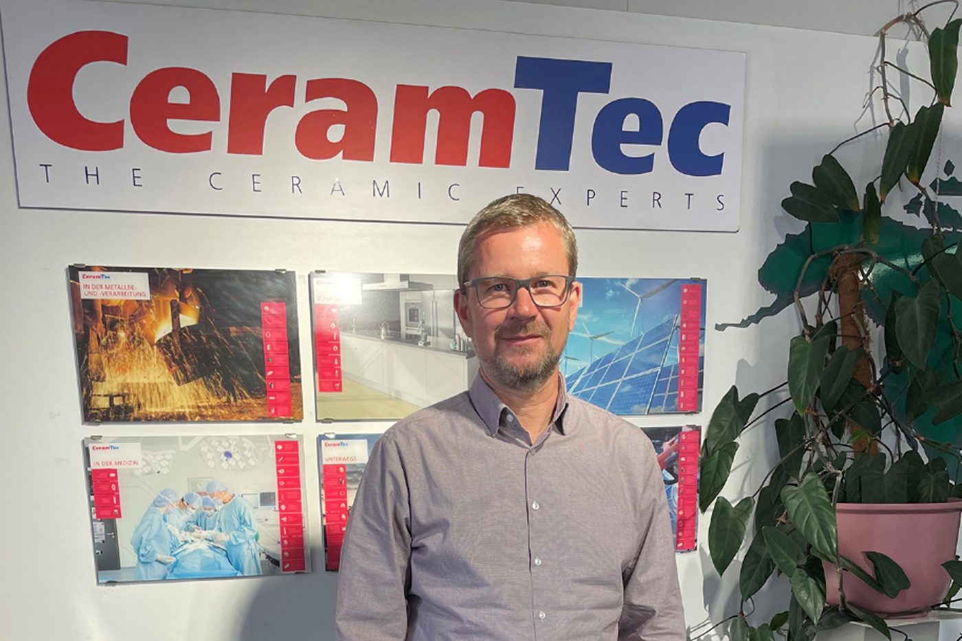
Author
Claus Falkner
Head of Tool Shop, CeramTec
Lauf, Germany